Customer First
We strive to understand our customers' processes and requirements, working collaboratively to ensure our carriers deliver measurable value in your specific application.
Patent pending temporary bonding technology, designed and manufactured in the United States.
Who We Are
Semi-Bond, LLC specializes in designing and manufacturing mobile temporary bonding and debonding carriers for the semiconductor and advanced packaging industries.
Our patent pending technology delivers zero-force release, wide operational envelopes, and bonds strong enough to hold even the smallest devices through demanding process steps. Every carrier is designed and built in the United States. We work with commercial semiconductor manufacturers, university research programs, and government-funded labs — wherever process teams need a reliable, low-overhead temporary bonding solution.
Our Commitment
We strive to understand our customers' processes and requirements, working collaboratively to ensure our carriers deliver measurable value in your specific application.
Our patent pending zero-force bond and debond technology enables ultra-strong bonds and reliable release without mechanical stress to devices or substrates.
All Semi-Bond products are designed and manufactured in the United States. This matters in practical terms for government contractors, national laboratories, defense-related programs, and organizations operating under domestic sourcing requirements — including those tied to CHIPS Act-funded initiatives.
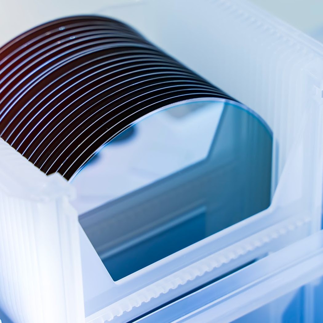
Carriers are available in standard wafer diameters as well as customer-defined shapes and sizes to accommodate virtually any semiconductor or packaging geometry.
Our carriers hold even the smallest devices securely throughout demanding semiconductor and packaging process steps, across wide ranges of temperature and chemical environments.
Semi-Bond carriers work in both wet and dry semiconductor processes and bond to almost any substrate.