Competitive Total Cost of Ownership
Semi-Bond carriers cost a fraction of competing temporary bonding solutions. No specialized equipment to buy, no lengthy prep steps, and faster cycle times add up quickly.
Engineered for the semiconductor and advanced packaging industries. Zero-force release. No support equipment. Made in the USA.
Product Overview
Semi-Bond carriers integrate directly into your existing processes with no support equipment required, at a fraction of the cost of electrostatic or adhesive bonding solutions.
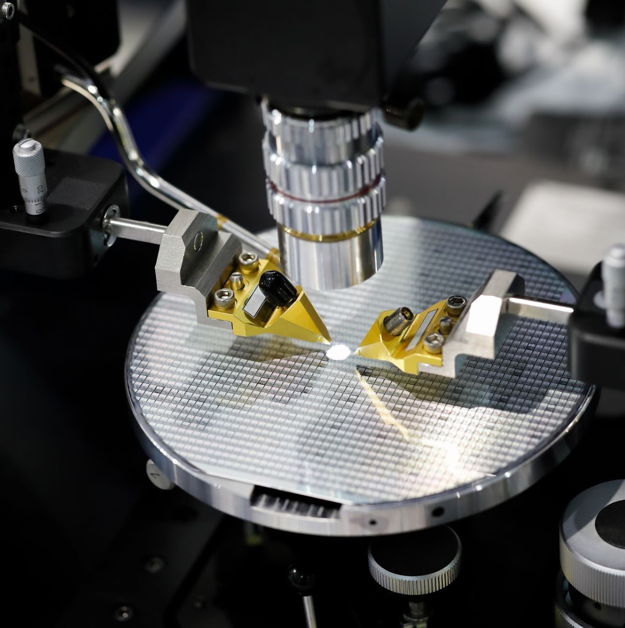
Our flagship product, the SBC-LT Series Carrier, is delivered fully prepared for bonding and debonding — no spin coat, bake, or cure of bonding material required. Each carrier supports tens of bond and debond cycles and is functional at operational temperatures of 250°C and above.
Semi-Bond carriers cost a fraction of competing temporary bonding solutions. No specialized equipment to buy, no lengthy prep steps, and faster cycle times add up quickly.
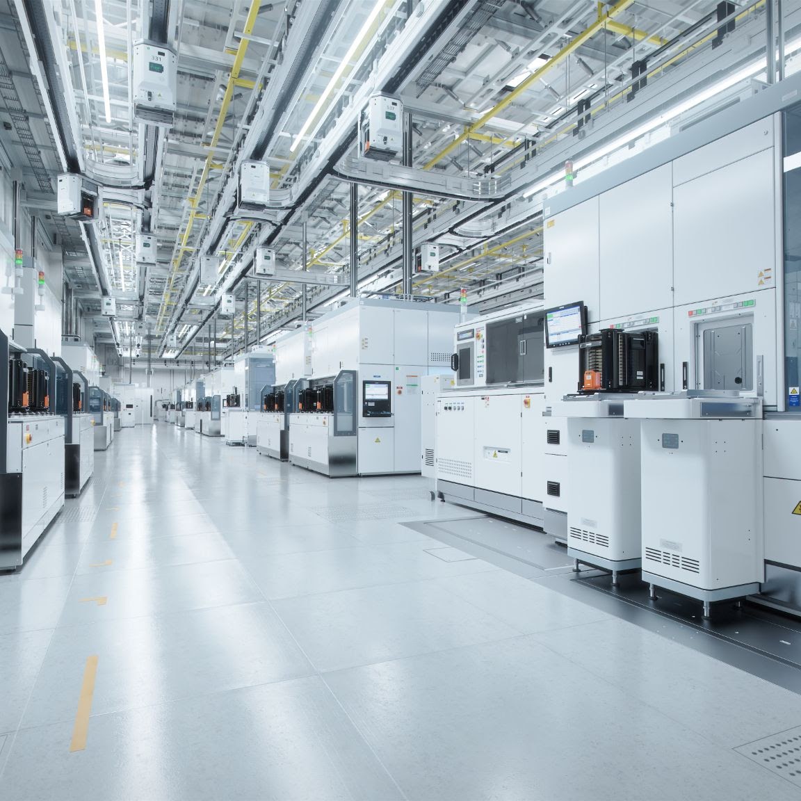
Our carriers drop into your existing semiconductor fabrication and advanced packaging processes. No additional handling equipment or processing tools to procure or qualify.
Bond and debond in seconds. No thermal slide, laser step, or chemical cleaning required.
Semi-Bond carriers work in both wet and dry semiconductor processes, covering a wide range of back-end-of-line and advanced packaging applications.
Zero-force bond and debond eliminates mechanical stress on devices and substrates, reducing the risk of damage or breakage throughout the process.
Our carriers maintain bond integrity at operational temperatures of 250°C and above, through wet processes, and under pressure — without bond degradation.
Semi-Bond carriers bond to almost any substrate, regardless of material or surface chemistry.
All Semi-Bond products are designed and manufactured in the USA, ensuring quality control, supply chain reliability, and domestic sourcing for customers who require it — including government contractors, national laboratories, and organizations operating under CHIPS Act or defense acquisition domestic sourcing requirements.
In Action

Custom Solutions
Semi-Bond carriers are available in standard wafer diameters and customer-defined shapes and sizes.